Views: 305 Author: Site Editor Publish Time: 2021-03-01 Origin: Site
The PCB circuit board market is constantly developing, mainly due to two forces. First, the market space of the PCB circuit board application industry continues to expand, and the communication industry and 5G industry have great room for application improvement. As a result, the multi-layer PCB circuit board market is also growing very rapidly, with the current application ratio reaching 50-60%. At the same time, the proportion of PCB circuit boards used in industrial electronic control, medical industry, and automotive electronics has also increased significantly, which has continued to expand the space of the PCB circuit board industry. Furthermore, the global PCB circuit board industry is moving to my country, which has also led to the rapid expansion of my country's PCB circuit board market space.
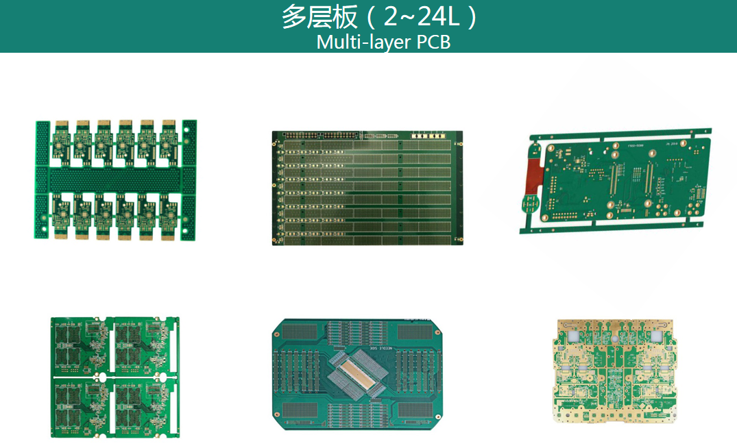
So in PCB circuit board design, process not only refers to the category of process data, but also refers to the manufacturer's capabilities. These data are based on the performance of the manufacturer's equipment and the overall design process. In the PCB circuit board process, three control points are particularly important: etching, drilling and positioning, but other properties will also affect the entire process category. As the technology upgrades, the technology categories are also differentiated, and the regulations of the technology categories will also change accordingly. PCB circuit boards are divided into single-sided PCB circuit boards, double-sided PCB circuit boards and multi-layer PCB circuit boards. Multi-layer PCB circuit boards refer to circuit boards with three or more layers. The manufacturing process of multi-layer PCB circuit boards will add the inner layer lamination manufacturing process on the basis of single and double panels. Distractions can also be analyzed using slices. Multi-layer PCB circuit boards are generally made of epoxy glass cloth-clad copper foil laminates, and their manufacturing process is developed based on the process of double-sided circuit boards with plated holes.
The process flow of multi-layer PCB circuit boards is to first etch the pattern of the inner layer board, and after blackening treatment, add prepreg sheets according to the predetermined design for lamination, then place a piece of copper foil on the upper and lower surfaces respectively, and send it to the laminating machine for heating and pressure to obtain a 'double-sided copper-clad board' with the inner layer pattern prepared. Then perform CNC drilling according to the pre-designed positioning system. After drilling, the hole wall must be etched and the drilling dirt removed, and then the following process operations can be carried out according to the double-sided plated hole circuit board process.